Note : Les descriptions sont présentées dans la langue officielle dans laquelle elles ont été soumises.
2126468
This invention relates to microwave bandpass
filters and more particularly to planar dual-mode
filters having patch resonators where the filter is
implemented using stripline or microstrip and to
bandpass filters where one or more resonators are
separated from one another within a compartmentalized
housing.
It is known to have dual-mode filters where
the filter has a plurality of s~uare or circular-
shaped resonators (often referred to as "cavities")with each resonator carrying two orthogonal modes
coupled by a structural disc continuity at 45O. One
such filter is described in Atia, et al., U.S. Patent
Number 5,268,659 entitled "Cononical Dual-Mode Filter"
issued November, 1977.
The use of two degenerate modes in
microstrip rings and patches to realize dual-mode
resonators is known (see a book entitled "Planar
Circuits for Microwaves and Light Waves" by T. Okoshi,
published in 1985 by Springer-Verlag, pages 36 to 39).
See also an article by Wolf entitled "Microstrip
Bandpass Filters Using Degenerate Modes of a
Microstrip Ring Resonator", Electron LETT, 1972, pages
163 and 164 and further a book entitled "Handbook of
Microstrip Antennas" by James, et al., published by
Peter Peregrinus Ltd. in 1989, pages 221, 222 and 273.
Dual-mode filters made from ring resonators are
described in Griffin, et al., U.S. Patent Number
4,488,131 entitled "MIC Dual-Mode Ring Resonator
Filter" and in an article by Guglielmi entitled
"Microstrip Ring Resonator Dual-Mode Filters"
distributed at a workshop on microwave filters for
space applications by European Space Agency/ESTEC in
June of 1991. This prior patent and articles describe
2126468
-
dual-mode microstrip resonator filters having a
structural discontinuity at a 45O angle to the two
orthogonal modes.
Fiedziuszko, et al., U.S. Patent Number
5,136,268 describes a dual-mode planar filter having
two or more resonators with a coupling path between
resonators being straight or curved, a width of the
coupling path being constant over its entire length.
The resonators are square resonators with one corner
cut-away at a 45 angle to introduce a structural
discontinuity. The Fiedziuszko, et al., U.S. Patent
Number 5,172,084 describes a planar dual-mode filter
having circular resonators.
A major concern with known patch resonator
filters is the difficulty in eliminating undesired
coupling between patch resonators that are not
interconnected by a coupling path. When this
undesirable coupling occurs, the filters cannot be
made to realize symmetrical frequency characteristics.
Further, known patch resonator filters permit the
realization of a relatively narrow bandwidth; or, they
have a relatively high loss performance; or, they
require the use of tuning elements to achieve the
desired coupling.
It is an ob ect of the present invention to
provide a dual-mode patch resonator filter that can be
used for conventional room temperature applications or
can be constructed of high temperature superconductive
films for cryogenic applications. It is a further
object of the present invention to provide a dual-mode
patch resonator filter that can be made to realize a
relatively wide bandwidth with superior loss
performance, without tuning elements, the patch
resonators being arranged to eliminate undesired
-- 2
2126~68
coupling between both adjacent and non-adjacent patch
resonators.
A bandpass filter in accordance with the
present invention includes a plurality of patch
resonators in a planar configuration where each
resonator has a periphery with perturbation means
thereon. The filter has a first coupling path
extending between two of said resonators, said
coupling path having two ends, each with a
substantially perpendicular end portion. The end
portions are substantially parallel to and spaced
apart from an adjacent section of said periphery of
the resonator located immediately adjacent to said end
portion. The filter has a housing and an input and
output.
In a further embodiment of the invention, a
bandpass filter includes a plurality of patch
resonators arranged in a planar configuration. Each
resonator has a periphery with perturbation means
located thereon. Each resonator is mounted in a
housing with separation means being located between a
first resonator and a second resonator to prevent
undesirable coupling between said first and second
resonators. The resonators are part of a circuit
extending between an input and an output of said
filter.
In the drawings:
Figure 1 is an exploded perspective view of
a four-pole dual-mode bandpass microstrip filter;
Figure 2 is a perspective view of a circuit
of the filter of Figure l;
Figure 3 is a schematic top view of a
coupling mechanism for the filter shown in Figure l;
-- 3
2126~68
Figure 4 is a graph showing the insertion
loss and return loss for a four-pole filter
constructed as shown in Figure 1;
Figure 5 is a perspective view of a
variation of a four-pole dual-mode circuit that can be
used in a filter in place of the circuit shown in
Figure 2 to realize an elliptic function filter or a
linear phase filter;
Figure 6 is a graph showing the insertion
loss and return loss of a four-pole filter using the
dual-mode circuit shown in Figure 5;
Figure 7 is a perspective view of a further
variation of a four-pole dual-mode circuit that can be
used in a filter in place of the circuit shown in
Figure 2;
Figure 8 is a perspective view of a
variation of the circuit shown in Figure 7 with a
change in location of a perturbation;
Figure 9 is an exploded perspective view of
an eight-pole dual-mode filter having two circuits
containing two resonators each where each circuit is
in a different compartment of a housing;
Figure 10 is a top view of the circuits of
the filter of Figure 9 assembled in a housing with a
cover removed;
Figure 11 is an exploded perspective view of
a further embodiment of an eight-pole dual-mode filter
where each resonator is located in a different circuit
and in a different compartment of a housing;
Figure 12 is a top view of an assembled
filter in accordance with Figure 11 with a cover
removed;
-- 4
2126468
Figure 13 is a graph showing the insertion
loss and return loss for an eight-pole filter having a
design similar to that shown in Figures 11 and 12;
Figure 14 is a top view of a variation of
the assembled filter of Figure 13 with the cover
removed; and
Figure 15 is an exploded perspective view of
a filter having four resonators with each resonator
being in a separate compartment of a housing and the
circuit being in one piece.
The filters of the present invention can be
implemented in microstrip and can be realized using
gold films for conventional room temperature
applications or using newly developed high temperature
superconductive films for cryogenic applications.
When the word "microstrip" is used in this
specification, it shall be interpreted to include
stripline or variations thereof.
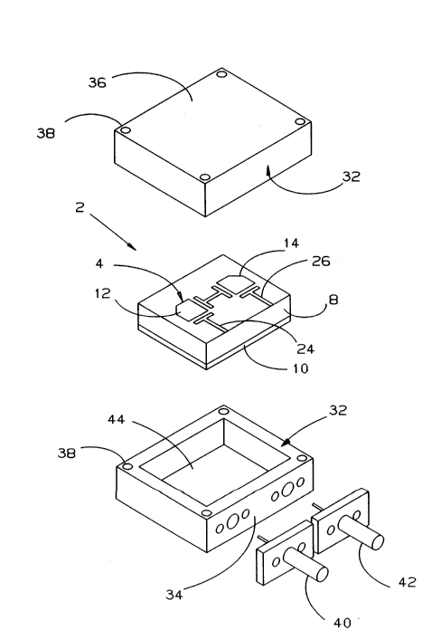
In Figures 1 and 2, a filter 2 has a circuit
4 printed on a top surface 6 of a substrate 8. A
bottom surface (not shown) of the substrate 8 is
covered by a metallization layer 10. The circuit 4
has two patch rectangular resonators 12, 14 separated
by a coupling path 16. The coupling path 16 is
substantially perpendicular to inner edges 18 of each
of the resonators 12, 14. Each end of the coupling
path 16 has a T-shaped end portion 20 that is
substantially perpendicular to the coupling path 16 in
an area of said end. The end portions 20 are
substantially parallel to, but separated from inner
edges 18 of each of the resonators 12, 14. Each patch
resonator 12, 14 has perturbation means 22 located
thereon. The perturbation means 22 is a perturbation
located at an outer corner of each resonator 12, 14.
-- S --
2126468
-
The perturbation means 22 can be located at other
corners of the patch resonators 12, 14 as well and can
have a different shape than that shown in Figure 1.
The perturbation means 22 is a cut-off corner at an
angle of 45 to edges of the resonators 12, 14.
An input line 24 is parallel to an output
line 26. The lines 24, 26 each have one end portion
28 that is substantially perpendicular to the lines
24, 26 and substantially parallel to an edge 30 of the
resonators 12, 14. The end portions 28 give the input
and output lines 24, 26 a T-shape. The T-shaped end
portions 28 may be omitted or replaced with various
other shapes as will be readily apparent to those
skilled in the art. The input line 24 and the output
line 26 form part of the circuit 4. The perturbation
means 22 is shown to be at an angle of 45 to each
mode axis of said filter but other angles will be
suitable.
The substrate 8 and the circuit 4 are
located within a housing 32 having a base 34 and a
cover 36. The base and cover each have suitable
openings 38 located therein so that the cover can be
tightly screwed or bolted onto the base 34 with the
substrate 8 located therein. The screws or bolts used
to affix the cover 36 to the base 34 are conventional
and are not shown. The housing can be made of any
known metallic materials or any non-metal that is
coated with metallic material. The housing 32 has an
input probe 40 and an output probe 42 connected
thereto. Patch resonator 12 supports first and second
degenerate modes while patch resonator 14 supports
third and fourth degenerate modes. The input line 24
and output line 26 are connected directly to the input
40 and output 42 respectively. Coupling between the
- 6 -
2126468
-
second mode of patch resonator 12 and the third mode
of patch resonator 14 is provided by the coupling path
16 and T-shaped end portions 20.
The various components of a circuit (for
example, the circuit 4) as well as the metallization
layer -(for example, the layer 10) can be made of any
known metals, including gold, silver, calcium and
copper or they could be made of superconductors or
they could be made of ceramic materials, including
YBCO (i.e. Yittrium Barium Copper Oxide) and TBCCO
(i.e. Thallium Barium Calcium Copper Oxide) which
become superconductors at cryogenic temperatures. The
substrate 8 can be made of any known dielectric
material, including alumina, lanthanum aluminate and
sapphire. The substrate 8 is affixed to the base 34
by various means including an adhesive, for example,
epoxy, between the ground plate 10 and an interior
surface 44 of the base 34.
Figure 3 shows a schematic version of part
of the circuit 4 of Figure 1. A value of the RF (i.e.
radio frequency) coupling to a patch resonator 46 by a
coupling path 48 having an end portion 50 can be
varied by adjusting the following four parameters:
(i) a gap width W between the end portion 50
and an inner edge 52 of the resonator 46;
(ii) a length L of a T-shaped end portion 50;
(iii) a thickness Wl of the end portion 50; and
(iv) a thickness W2 Of the coupling path 48.
The T-shaped coupling mechanism shown in
Figure 3 results in larger coupling values being
attainable than with previous devices. The larger
coupling values allow the realization of a relatively
wider bandwidth filter than would be attainable
without the coupling mechanism (i.e. without the end
-- 7
2126468
portion 50). In addition, in the arrangement shown in
Figure 2, the coupling mechanism allows coupling
between the second and third modes but will not permit
coupling between the first and fourth modes.
In Figure 4, the insertion loss and return
loss results of a four-pole filter constructed in
accordance with Figure 1 are shown. A gold film was
printed onto a lanthanum aluminate substrate. The
coupling path between the resonators permits coupling
between the second and third modes and the filter
realizes a Chebyshev filter response (i.e. the
coupling path will not permit the creation of
undesired coupling between the first and fourth
modes). No tuning elements were used to attain the
results shown in Figure 4.
In Figure 5, there is shown a circuit 54
that is a variation of the circuit 4 shown in Figures
1 and 2. The same reference numerals are used in
Figure 4 as are used in Figures 1 and 2 to refer to
the same components. The particular circuit 54 has an
additional coupling path 56 extending between the
patch resonators 12, 14 and includes the coupling
paths 16, 56, the resonators 12, 14 and the input and
output lines 24, 26. The additional coupling path 56
is U-shaped with T-shaped end portions 58 located
adjacent to, but spaced apart from, each of the
resonators 12, 14. The T-shaped end portions 58 are
substantially perpendicuIar to the conducting path in
an area of the ends of said coupling path. The
additional coupling path 56 provides an additional
coupling between a first mode of patch resonator 12
and a fourth mode of patch resonator 14. The circuit
54 can be used to realize an elliptic function filter
or a linear phase filter. While the additional
-- 8 --
2126468
_
coupling path 56 is shown as being U-shaped, other
shapes will be suitable as well. When the circuit 54
is used in an elliptic function filter, the additional
coupling carried out through path 56 should be
negative. The coupling value through the path 56 and
whether the coupling is positive or negative can be
controlled by adjusting the length of the U-shaped
path in addition to adjusting the four parameters W,
Wl, W2 and L described in Figure 3.
In Figure 6, there is shown the insertion
loss and return loss for the four-pole filter using
the circuit 54 of Figure 5. The dimensions of the
coupling elements are chosen to produce a negative
coupling between the first mode of the resonator 12
and the fourth mode of the resonator 14. These
results were produced without the use of any tuning
mechanism in the filter utilizing the circuit 54.
Figure 7 shows a further variation of the
circuit 4 of Figure 1 and the circuit 54 of Figure 4.
The same reference numerals used in Figures 1 and 4
are used in Figure 5 for the same components. In
Figure 7, a circuit 60 has a U-shaped coupling path 56
as shown in Figure 5 extending between the resonators
12, 14, but the coupling path 16 of Figure 5 has been
omitted. The circuit 60 includes the resonators, the
coupling path and the input lines and output lines.
Coupling between the second mode of patch resonator 12
and the third mode of patch resonator 14 is provided
through a gap G, being a perpendicular distance
between the resonators 12, 14. An advantage of the
gap coupling mechanism is that the patch resonators
12, 14 can be brought closer together which can result
in an overall smaller filter structure than that shown
in Figures 1 and 5. The gap coupling mechanism
_ 9 _
212~68
results in undesired coupling between the first mode
of patch resonator 12 and the fourth mode of patch
resonator 14. This undesired coupling can be
controlled by adding the coupling path 56. The
coupling between the first and fourth modes can be
adjusted to zero (for Chebyshev realization), or to a
positive value (for linear phase realization), or to a
negative value (for elliptic function realization).
In Figure 7, it should be noted that the perturbation
means 22 or corner cut for each of the resonators 12,
14 is located so that the undesired coupling between
the first and fourth modes will have a positive value.
In Figure 8, a circuit 62 is identical to
the circuit 60 of Figure 7 except that a perturbation
means-64 or corner cut of the patch resonator 12 is
located on an inside corner adjacent to the coupling
path 56 rather than an outside corner 22 as previously
shown in Figure 7. The perturbation means or corner
cut of the patch resonator 14 is unchanged from that
shown in Figure 7. The undesired coupling between the
first mode of the resonator 12 and the fourth mode of
the resonator 14 is made negative by the location of
the corner cut 64 as shown in Figure 8. The same
reference numerals have been used to describe the same
components in Figures 7 and 8. The overall coupling
between the first and fourth modes can be adjusted to
be positive, zero or negative, as desired, with the
circuit 62 shown in Figure 8 by utilizing the coupling
path 56 and end portions 58.
In Figures 9 and 10, there is shown an
exploded perspective view of an eight-pole dual-mode
filter 65 having three partial circuits 66, 68, 70
mounted in a compartmentalized housing 72 having a
base 74 and a cover 75. The partial circuits 66, 68,
- 10 -
2126~68
-
70 together constitute the circuit for the filter 65.
The base 74 of the housing 72 has two compartments 76,
78 that are separated by two septa 80, 82. The septa
80, 82 are separated by an aperture 84 into which is
inserted the partial circuit 68. The partial circuits
66, 70 are inserted into the compartments 76, 78
respectively. The housing 72 has an input 86 and an
output 88. The partial circuits 66, 70 are generally
mirror images of one another and each of said circuits
is generally identical to the circuit 54 of Figure 5
except for the angle of an input path 90 and an output
path 92.
While the partial circuits 66, 70 have
generally the same shape, the four parameters W, L,
1, W2, described with respect to Figure 3 may vary
between the partial circuit 66 and the partial circuit
70. Those variations may apply between all circuits
of the present application where it is stated that two
or more circuits are "generally mirror images" or are
"generally identical" or similar variations of those
phrases. The partial circuits 66, 68, 70 have a
substrate 94 and a metallization layer 96 (not shown
for the circuit 68). The assembled version of the
partial circuits 66, 68, 70 in the base 74 of the
housing 72 is shown in Figure 10. The input 86 and
output 88 are two connectors that have inner
conductors 98, 100 that are connected to the two
partial circuits 66, 70 respectively. While the
substrate 94 and metallization layer 96 for each of
the partial circuits is cut so that each partial
circuit is a separate piece, the partial circuits can
be formed on one substrate and one metallization layer
which can be cut so that the circuit is in one piece
only or in two pieces only.
- 11 -
2126~68
With continuing reference to Figure 10, in
operation, RF energy is coupled to the filter 65
through the input 86 and through the input path 90 and
a T-shaped end portion 102 to a patch resonator 104.
Coupling between a second mode of resonator 104 and a
third mode of a resonator 106 of the partial circuit
66 is provided by a coupling path 108 and two T-shaped
end portions 110. Coupling between a first mode of
the resonator 104 and a fourth mode of the resonator
106 is provided through a U-shaped coupling path 112
with T-shaped end portions 114. Coupling between the
fourth mode of the resonator 106 of the partial
circuit 66 and a fifth mode of a resonator 116 of the
partial circuit 70 is provided by interconnecting an
output path 118 and T-shaped end portions 120 of the
partial circuit 66 through the partial circuit 68 to
an input path 122 and T-shaped end portion 124.
Interconnects 126, 128 to and from the partial circuit
68 can be of various known forms for line
interconnects including ribbon bonding, wire bonding
and epoxying. When the circuit is one piece, the
interconnects can be eliminated. A coupling path 130
and T-shaped end portion 132 of the partial circuit 70
provide coupling between a sixth mode of the resonator
116 and a seventh mode of the resonator 134 of the
partial circuit 70. A coupling path 136 and T-shaped
end portions 138 of the partial circuit 70 provide
coupling between a fifth mode of the resonator 116 and
an eighth mode of the resonator 134 of the partial
circuit 70. The RF energy is coupled out of the
filter through the output path 92 and a T-shaped end
portion 136 to the output 88.
The septa 80, 82 eliminate undesired
coupling between patch resonator 104 of partial
- 12 -
2126~68
`_
circuit 66 and patch resonators 116, 134 of partialcircuit 70. Similarly, the septa 80, 82 eliminate
undesired coupling between patch resonator 134 of the
partial circuit 70 and patch resonators 104, 106 of
the partial circuit 66. The septa 80, 82 also help to
eliminate undesired waveguide modes that might
propagate in the filter if the septa were removed.
In Figure 11, there is shown an exploded
perspective view of an eight-pole filter 140 having
partial circuits 142, 144, 146, 148, 150, 152, 154
that together constitute one circuit. The four
partial circuits 142, 146, 150, 154 are generally
identical to one another and the partial circuits 144,
148, 152 are generally identical to one another. Each
partial circuit has a substrate 94 and a metallization
layer 96. The filter 140 has a compartmentalized
housing 156 with a base 158 and a cover 160. The base
of the housing has four compartments 162, 164, 166,
168. The four compartments are created by septa 170,
172, 174, 176, 178. The septa 170, 172 are separated
by an aperture 179 between the compartments 162, 164.
The septa 174, 176 are separated by an aperture 180
between the compartments 164, 166. The septa 172, 174
are separated by an aperture 182 between the
compartments 166, 168. The filter 140 has an input
184 and an output 186 having connectors 188, 190. The
input 184 and output 186 are connected through the
housing in a similar manner as the input 86 and output
88 of the filter 65 shown in Figures 9 and 10.
In Figure 12, the filter 140 is shown
assembled within the base 158 of the housing 156 with
the cover (not shown) removed. Each of the partial
circuits 142, 146, 150, 154 has a patch resonator
192a, 192b, 192c, 192d, one T-shaped input line 194a,
- 13 -
2126~68
194b, 194c, 194d and one T-shaped output line 196a,
196b, 196c, 196d respectively. Energy is coupled
through the three partial circuits 144, 148, 152 by
interconnects 126, 128. The base 158 and cover 160
contain suitable openings 38 to receive screws or
bolts (not shown) so that the cover 160 can be
securely attached to the base 158.
Figure 13 shows the return loss and
insertion loss for an eight-pole filter that is
designed similarly to the filter shown in Figures 11
and 12, except for the results shown in Figure 13, the
coupling paths 112, 136 have been removed from each of
the circuits 66, 70 to produce a Chebyshev response.
Also, for the results shown in Figure 13, the circuit
was made of a single-sided high temperature
superconductive wafer that becomes a superconductor at
cryogenic temperatures. No tuning elements were used
to achieve the performance shown in Figure 13.
While each resonator 192 of the filter 140
can be made to resonate in a dual-mode so that the
filter functions as an eight-pole filter, the
resonators can also be made to resonate in a single
mode so that the filter functions as a four-pole
filter.
In operation, energy is coupled through the
input 184 into the partial circuit 142 through the
input line 194a to the resonator 192a and out of the
resonator 192a, through the output line 196a, through
the partial circuit 144 and into the input line 194b
of the partial circuit 146. Energy is coupled into
the resonator 192b and out of the resonator 192b,
through the output line 196b and through the partial
circuit 148, to the input line 194c of the partial
circuit 150. Energy is coupled from the input line
- 14 -
2126468
-
194c into the resonator 192c and out of the resonator
192c to the output line 196c. From the output line
196c, energy is coupled through the partial circuit
lS2 into the input line 194d of the partial circuit
154 to the resonator 192d and to the output line 196d
of the partial circuit 154. Energy is coupled from
the output line 196d of the partial circuit 154
through the partial circuit 118 to the output 186. It
can be seen that the output 196a, partial circuit 144
and input 194b form an I-shaped coupling path between
the resonators 192a and 192b. Similarly, the output
196b, partial circuit 148 and input 194c form an I-
shaped coupling path between the resonators 192b and
192c and the output 196c, partial circuit 152 and
input 192d form an I-shaped coupling path between the
resonators 192c and 192d.
In dual-mode operation, energy is coupled
from the first mode to the second mode in the
resonator 192a of the partial circuit 142. Energy is
coupled from the second mode of the resonator 192a of
the partial circuit 142 to the third mode of the
resonator 192b of the partial circuit 146. Energy is
coupled from the third mode to the fourth mode in the
resonator 192b of the partial circuit 146. Energy is
coupled from the fourth mode of the partial circuit
146 to the fifth mode of the resonator 192c of the
partial circuit 150. Energy is coupled from the fifth
mode to the sixth mode in the resonator 192c of the
partial circuit 150 and from the sixth mode to the
seventh mode in the resonator 192d of the partial
circuit 154. Energy is coupled from the seventh mode
to the eighth mode of the resonator 192d in the
partial circuit 154 and from the eighth mode to the
output 186. The filter 140 can be operated as an
- 15 -
2126468
_
eight-pole filter with quasi-elliptic or self-
equalized functions.
In Figure 14, there is shown a top view of a
filter 200 having four patch resonators 202a, 202b,
202c and 202d, each resonator being part of a partial
circuit 204a, 204b, 204c, 204d where each partial
circuit is mounted in a different compartment of a
housing 206. Only the base 208 of the housing 206 is
shown in Figure 14 as the cover (not shown) is
removed. The filter 200 has a physical structure that
is almost identical to the filter 140 shown in Figures
12 and 13. The same reference numerals have been used
in Figure 14 for those components that are virtually
the same as those shown in Figures 12 and 13. The
patch resonators 202a, 202b, 202c, 202d each have
perturbation means 210 at an inner corner thereof. In
addition, the partial circuits 204a, 204d are
generally mirror images of one another and have a
partial T-shaped coupling path 212a, 212d that extends
to resonators 202b, 202c respectively. Partial
circuits 204b, 204c are generally mirror images of one
another and each of these circuits has two T-shaped
coupling paths 212b, 212b', 212c, 212c' respectively
that extend toward resonators in adjacent cavities.
Three additional partial circuits 214 are mounted in
apertures (not shown). The partial circuits 204a,
204b, 204c, 204d, 144, 148, 152, 214 constitute the
circuit for the filter 200. The filter has an input
184 and an output 186. The housing 206 is divided
into four compartments by septa 216, 218, 220, 222,
224, 226, 228, 230.
In dual-mode operation of the filter 200, RF
energy is coupled into the resonator 202a through the
input 184 and the input line 194a. Coupling between a
- 16 -
- 2126~58
second mode of the resonator 202a and a third mode of
the resonator 202b is provided by output line 196a,
partial circuit 144 and input line 194b, which
together form an I-shaped coupling path. The partial
circuit 144 is connected to the output line 196a by
interconnect 126 and to the input line 194b by the
interconnect 128. The interconnects 126, 128 are in
all of the coupling paths of the filter 200 when the
coupling path extends from one compartment of the
housing to another. The interconnects will not be
specifically discussed for the remaining coupling
paths. Coupling between a first mode of the resonator
202a and a fourth mode of the resonator 202b is
provided through output line 204a, partial circuit 214
and input line 212b, which together form a U-shaped
coupling path. Coupling between the fourth mode of
the resonator 202b and a fifth mode of the resonator
202c is provided through output line 196b, circuit 148
and input line 194c, which together form an I-shaped
coupling path. Coupling between the third mode of the
resonator 202b and a sixth mode of the resonator 202c
is provided through output line 212b', circuit 214 and
input line 212c, which together form a U-shaped
coupling path. Coupling between the sixth mode of the
resonator 202c and a seventh mode of the resonator
202d is provided through output line 196c, circuit 152
and input line 194d, which together form an I-shaped
coupling path between the resonators 202c and 202d.
Coupling between the fifth mode of the resonator 202c
and an eighth mode of the resonator 202d is provided
through output line 212c', circuit 214 and input line
212d, which together form a U-shaped coupling path
between the resonators 202c and 202d. Energy is
coupled out of the filter 200 through the output line
- 17 -
2126468
196d and the output 186. The input 184 and the output186 are probes.
In Figure 15, there is shown a filter 232
which is a variation of the filter 140 shown in
Figures 12 and 13. Those components of the filter 232
that are essentially the same as the components of the
filter 140 are identified with the same reference
numerals. The housing 156 and the input 184 and
output 186 are identical to those of the filter 140.
The filter 232 has a circuit 234 that is formed on a
single substrate 236 having a single metallization
layer 238. The circuit 234, substrate 236 and
metallization layer 238 are cut in a single piece that
is shaped to fit within the base 158 of the housing
156 so that there is one resonator 192a, 192b, 192c,
192d in each compartment 162, 164, 166, 168
respectively. The circuit 234 has the input line 194a
and the output line 196d. There is an I-shaped
coupling path 240 between the resonators 192a and
192b. There is an I-shaped coupling path 242 between
the resonators 192b and 192c and an I-shaped coupling
path 244 between the resonators 192c and 192d. Since
the circuit 234, substrate 236 and metallization layer
238 are cut in one piece, the interconnects 126, 128
shown in Figure 13 for the filter 140 are not
required. The circuit 234, substrate 236 and
metallization layer 238 are cut in one piece so that
they fit properly between the septa in the base 158 of
the housing 156 with the I-shaped coupling paths 240,
242, 244 extending through the apertures 179, 180,
182. The filter 234 operates in the same manner as
the filter 140 but has a better insertion loss
performance and is easier to assemble. While the
circuit of the filter 140 has seven separate pieces
- 18 -
2126~68
_
(of partial circuit) that must be assembled into thehousing, the circuit 234 of the filter 232 has only
one piece. As a further variation, a filter could be
constructed where the circuit, substrate and
metallization layer are cut into more than one piece
but less than seven pieces. Still further, a circuit
could be formed on a substrate and metallization layer
that has a pre-existing shape to conform to the
arrangement of septa and apertures within a housing so
that it is not necessary to cut the substrate and
metallization layer at all.
While the present invention has been fully
described and a preferred embodiment has been set out,
there are numerous variations and modifications that
can be made to the invention within the scope of the
attached claims by those skilled in the art. For
example, the input line and output line and/or the
coupling path or end portions could be L-shaped rather
than T-shaped. As another example, the I-shaped
coupling paths could be used to act as resonant
elements. The dimensions of the I-shaped coupling
path in Figure 2 could be chosen to realize a five-
pole Chebyshev filter rather than a four-pole
Chebyshev filter. In this arrangement, the two T-
shaped input and output lines 24, 26 will provide thenecessary coupling between the two patch resonators
12, 14 and the resonant line of I-shaped coupling path
16, 20.
As yet another example of variations that
can be utilized, when the circuits are used in a
compartmentalized housing, two or more of the partial
circuits or even all of the partial circuits for any
filter could be formed in one piece for insertion into
the base of the housing. For example, for the filter
- 19 -
2126468
65 of Figure 9, the partial circuits 66, 68, 70 as
well as the substrate 94 and metallization layer 96
for each of these partial circuits could be formed in
one piece. The substrate and metallization layer
could then be cut-away between the partial circuits
66, 70 up to the partial circuit 68 so that the
substrate and metallization layer for the two partial
circuits 66, 70 would remain joined by the circuit 68
into one piece. That one piece would then be inserted
into the housing. In this arrangement, the
interconnects 126, 128 could be eliminated as the
circuit 68 would not be a separate piece but would be
connected directly to the circuit 66, 70. The same
one piece circuit arrangement could be utilized for
the filter 200 of Figure 14 or for other filters that
are within the scope of the attached claims. For the
filter 140, the partial circuits 142, 146, 150, 154
would be interconnected by one substrate 94 and one
metallization layer 96 that was cut in such a way that
the filter would fit into the base 158 of the housing
156. In place of a compartmentalized housing for a
filter, separate housings can be utilized.
- 20 -