Note: Descriptions are shown in the official language in which they were submitted.
CA 02571700 2006-12-19
Method and System of Combining Signals in BPL Communications
Field of the Invention
The invention relates to broadband over power line ("BPL") communications, and
more
particularly to such communications between a BPL modem and a medium voltage
("MV")
power line.
Background of the Invention
Using BPL communications on MV power lines requires repeating or regenerating
signals at
various intervals to maintain sufficient signal strength to reach the signal
destination. Such
signal regeneration may be done by BPL modems connected to the MV power line.
When
multiple devices try to communicate over a single physical line, the devices
must follow a
specified scheme to share the physical resource and to avoid interfering with
each other. There
are two such schemes commonly used, one referred to as Time Division Duplexing
("TDD"),
and the other as Frequency Division Duplexing ("FDD").
TDD is a scheme whereby devices split up a period of time T (seconds) into N
divisions, with
each device being given TIN (seconds) of the total time T in which to
communicate over the
single line. Each device waits for its specific time slot and when its turn
arrives, the device uses
the full frequency band available to communicate.
FDD is a scheme whereby devices split up the total frequency band F (measured
in Hertz), into
N divisions, with each device being given FIN (Hertz) of the total F band in
which to
communicate. Each device communicates as required (as opposed to TDD where a
device only
communicates in its own designated time division) but only in its allocated
frequency band (as
opposed to TDD where a device uses the full frequency band to communicate).
When using FDD (which is the most efficient way of building large networks)
BPL modems
require at least two internal modems and corresponding ports, one for upstream
communication
along the MV power line, and one for downstream communication along the MV
power line.
Each port is connected to a MV coupler used to couple the signal from the
internal modem to the
MV power line.
CA 02571700 2006-12-19
Figure 1 shows a typical BPL access system over MV power line 100 utilizing
FDD for
repeating the BPL signal. BPL modem 110 has two ports, 120 and 130, for input
and output, for
upstream and downstream communications, respectively. Each port 120, 130 is
connected to a
coupler 140, 150.
BPL modem 110 also acts as a repeater. BPL signal 1 is received and "repeated"
(i.e. the signal
is regenerated and retransmitted) and sent out as BPL signal 2 and vice versa.
BPL Modem 110
typically includes two internal modems (and may have more) for FDD repeating.
In FDD
communications, when the signal is repeated a different frequency band is used
for the upstream
and downstream directions of communication, respectively, but BPL modem 110 is
transmitting/receiving constantly (unlike TDD communications wherein a time
slot is assigned).
Summary of the Invention
The system and method according to the invention allows for a BPL MV
communications
system on power utility grid that eliminates the need for two MV couplers per
BPL modem (one
for each of two communication directions) when utilizing FDD. This is achieved
by combining
the upstream and downstream signal outputs from a BPL modem prior to coupling
to the MV
power line. The combining of the signals can occur internal or external to the
BPL modem.
The system and method according to the invention provides for fewer safety
concerns as linemen
interact less with the MV power lines (as they only attach one coupler). Such
MV power lines
have the potential to injure or kill a person.
The system and method according to the invention decreases the expense of
using two couplers
per modem, and provides for fewer points of failure and less time and cost to
install. As couplers
are similar in expense to BPL modem, the elimination of a coupler reduces the
deployment
hardware costs of a BPL system significantly (e.g. by 25-35%).
A method of communicating signals from a BPL modem to a medium voltage power
line, is
provided, including communicating a first signal for a medium voltage power
line from a first
signal source; communicating a second signal for the medium voltage power line
from a second
signal source; combining the first and second signals into a third signal
prior to the signals
2
reaching the medium voltage power line; and communicating the third signal to
the medium
voltage power line.
The first signal source may be a first internal modem within a BPL modern and
the second signal
source may be a second internal modem within the BPL modem. The first and
second signals
may be combined by a radio frequency ("RF") combiner.
The first signal may pass through a first RF filter prior to reaching the RF
combiner and the
second signal may pass through a second RF filter prior to reaching the RF
combiner. After
passing through the first RF filter, the first signal may have a first
allotted bandwidth and after
passing through the second RF filter, the second signal may have second
allotted bandwidth, the
first allotted bandwidth not overlapping with the second allotted bandwidth.
A system for communicating BPL signals is provided, including a BM, modem
having a first
internal modem and a second internal modem, the first internal modem and the
second internal
modem each in communication with a RF combiner; the RF combiner in
communication with a
medium voltage power line; and wherein the RF combiner combines signals from
the first
internal modem and the second internal modem into a third signal, and
communicates the third
signal to the medium voltage power line.
The first internal modem may communicate upstream signals and the second
internal modem
may communicate downstream signals. The system may include a first RF filter
in
communication with the first internal modem and the RF combiner and a second
RF filter in
communication with the second internal modem and the RF combiner. The first
signal may have
a first allotted bandwidth, wherein the first RF filter filters a first signal
from the first internal
modem to the first allotted bandwidth. The second signal may have a second
allotted bandwidth,
the first allotted bandwidth not overlapping with the second allotted
bandwidth, wherein the
second RF filter filters a second signal from the second internal modem to the
second allotted
bandwidth.
Brief Description of the Drawings
Figure I is a block diagram of a typical prior art BPL access system using two
MV couplers;
3
I URON110. 946236\1A (109637)
CA 2571700 2017-10-13
CA 02571700 2006-12-19
Figure 2 is a block diagram of a BPL access system using FDD with a single MV
coupler
according to the invention;
Figure 3 is a block diagram showing the combination of two different BPL
signals using FDD;
Figure 4 is a block diagram of a BPL modem;
Figure 5 is a block diagram of BPL internal signal reflection occurring within
a RF combiner;
Figure 6 is a block diagram of BPL external signal reflection occurring within
a RF combiner;
Figure 7 is a block diagram of internal signal leakage occurring within a RF
combiner; and
Figure 8 is a block diagram of a BPL access system according to the invention.
Detailed Description of the Invention
As shown in Figure 2, a BPL access system according to the invention,
generally designated as
10, communicating over MV power line 100 and using FDD to combine BPL Signal 1
and BPL
Signal 2 into BPL Signal 1 + 2, requires only one MV coupler 200, which
provides for both
upstream and downstream traffic along MV power line 100. BPL modem 210
therefore requires
only a single input/output port 220, in the case where RF combiner is internal
to BPL modem
210.
Figure 3 shows how BPL signal 1 and BPL signal 2 (one intended for upstream
communications,
the other for downstream) are combined into one signal, BPL Signal 1 + 2. As
BPL signal 1 and
BPL signal 2 are in different frequency bands according to FDD, they can be
combined with
minimal interference. RF combiner 300 is used to combine BPL signal 1 and BPL
signal 2. RF
combiner 300 can be an off the shelf component (when external to modem 210) or
can be
positioned within BPL modem 210.
As shown in Figure 4, BPL modem 210 may have multiple internal modems 400,
410, and 420,
within for upstream, downstream and other communications, such as low voltage
(LV) BPL
communications, and therefore multiple input/output ports 430, 440, and 450
corresponding to
each internal modem. Multiple internal modems 400, 410 and 420 allow BPL modem
210 to
4
CA 02571700 2006-12-19
function as a repeater as well as act as a source of, i.e. originate, and
receive BPL signals. BPL
modem 210 may have more or less internal modems and corresponding input/output
ports. The
signals from multiple input/output ports 430, 440 and 450 may be combined into
a single
input/output line if they use different frequency bands according to FDD. RF
filters 460, 470, as
seen in Figure 8, are used to ensure the frequency bands of each of internal
modem 400 and 410
do not overlap due to frequency response roll offs, i.e. slopes, that are
insufficiently steep.
Certain challenges are presented in combining signals in BPL communications,
including signal
reflections and signal isolation. Signal reflections occur when impedance
mismatches take place
on a MV power line, which occur when connecting devices, such as BPL modems,
to a MV
power line. Two types of signal reflections occur frequently within RF
combiners when
combining signals, as described below, and shown in Figures 5 and 6.
Another obstacle to signal combination is the need for signal isolation
between two input/output
ports 430, 440 of the modems 400 and 410, respectively, to prevent unwanted
signal leakage
from one port to the other. Figure 7 shows the potential signal leakage that
can occur within RF
combiner 500 without proper isolation between the two ports 430, 440.
Figure 5 shows BPL signal 1 entering RF combiner 500 from input/output port
430. RF
combiner 500 can be mounted internally or externally to BPL modem 210 and can
be part of the
circuit board to avoid having to use additional components. For BPL
communications, RF
combiner typically has a strong frequency response in the range of 1-40MHz,
although BPL
communications are not restricted to these frequencies and the frequency
response range could
be greater. A portion of BPL signal 1 is reflected back upon itself when it
reaches the physical
location point 510 where the signal combination occurs within RF combiner 500.
This signal
reflection acts as interference and significantly degrades the performance of
the BPL
communication system.
Figure 6 shows BPL signal 1 entering RF combiner 500 and then being reflected
back upon itself
when it reaches external device 600, which may be a MV coupler, a transformer
or other BPL
communications device. This signal reflection acts as interference and
significantly degrades the
performance of the BPL communication system.
5
Figure 7 shows BPI, signal 1 and BPL signal 2, from internal modem 400 and
410, respectively,
entering RF combiner 500, in which BPL signal 1 leaks back upon BPL signal 2's
path when
BPL signal 1 reaches the physical location point 510 where BPL signal 1
combines with BPL
signal 2. Likewise, BPL signal 2 enters combiner 500 and then leaks back upon
BPL signal l's
path when BPL signal 2 reaches the physical location point 510 where the BPL
signals 1 and 2
combine. This signal leakage acts as interference and significantly degrades
the performance of
the BPL communications system.
To prevent signal reflection and signal leakage there must be specific
attenuations introduced
within RF combiner 500 (regardless of whether combiner 500 is located internal
to or external
from BP modem 210). The attenuation to prevent reflections, as seen in Figures
5 and 6 and as
known in the art as "return loss", should be as large as possible (typically
25 dB or more to be
effective). The attenuation between input/output ports is known in the art as
"port to port
attenuation" or "port isolation" and should also be as large as possible
(typically 30 dB or more
to be effective).
Normal BPL signal flow (i.e. BPL Signal 1 and BPL Signal 2 and the combined
BPL Signal
1 + 2 traveling in both directions) is not attenuated, even in the presence of
high port isolation
and high return loss, as if BPL Signal 1 and BPL Signal 2 are attenuated, then
the transmission
power of these signals is reduced (and have a lower signal to noise ratio) and
the signals may
thus lose throughput. RF combiner 500 should therefore be selected or designed
with the above
attenuation specifications to provide maximum signal to noise ratio and
minimal interference.
A challenge in combining signals is thus minimizing interference between the
different signals,
BPL signal 1 and BPL signal 2, being combined. As seen in Figure 8, filters
460, 470 are used
for corresponding input/output ports 430, 440. Filters 460, 470 are RF filters
that are allotted a
particular frequency band (pursuant to FDD). For example, first internal modem
400 may be
designated to communicate within frequencies between 2-12 MHz and second
internal modem
410 may be designated to communicate within frequencies between 12-22 MHz, in
which case,
RF filters 460, 470 ensure that internal modems 400, 410 do not use
frequencies outside those
designated bands. Typical frequency bands may be 2-12, 13-23, or 24-34 MHz if
three frequency
modes are allotted. More or less frequency bands may be allotted and the
available bandwidth
6
TORONTO 946236\1A (109637)
CA 2571700 2017-10-13
CA 02571700 2006-12-19
may be broken up differently (for example the bandwidth split does not have to
evenly split the
entire bandwidth available). The frequency roll off on the RF filter should be
sufficiently steep
to ensure minimal out of band communications (e.g. an 8th order RF filter).
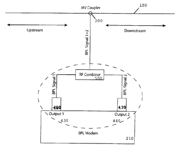
As seen in Figure 8, internal modems 400 and 410, are in communication with RF
combiner 500
via conventional wires or the like. RF combiner 500 is similarly in
communication MV power
line 100. RF filters 460, 470 receive communications from internal modems 400
and 410
respectively, and communicate the filtered communications to RF combiner 500.
Therefore, the
signals from internal modems 400, 410 pass through RF filters, 460, 470 before
arriving at RF
combiner 500. As shown by the dashed lines, RF combiner 500 and RF filters
460, 470 may be
to internal or external to BPL modem 210.
Signals communicated from the MV power line 100 through MV coupler 200 can be
separated.
Such signals will be filtered by RF filters 460, 470 for their respective
input/output ports 430,
440.
Although the particular preferred embodiments of the invention have been
disclosed in detail for
illustrative purposes, it will be recognized that variations or modifications
of the disclosed
apparatus lie within the scope of the present invention.
7