Note: Descriptions are shown in the official language in which they were submitted.
CA 02251517 1998-11-13
MICROWAVE SWITCH WITH MET'I-IOD OF OPERATION THEREOF
The present invention relates to microwave switches and, more
particularly, to the realisation of high temperature superconductive switches
and circuits.
5 The majority of communication systems utilise RF switches to achieve
dynamic interconnectivity or to improve system reliability by switching to
back-up equipment in case of a failure. The two types of switches that are
currently being used are electromechanical switches and solid state switches.
Electromechanical switches are usually used in applications where switching
to time can be slow while low insertion loss and high isolation are required.
The problem, however, with mechanical switches is that they are bulky.
Solid state switches, on the other hand, are used in applications where
switching time must be fast. Although, solid state switches are relatively
small in size and mass, their insertion loss performance and power
15 consumption are prohibitively high in many applications.
When working with HTS circuits difficulties have been encountered
in attempting to combine incompatible components with H'fS into the FITS
circuit. For example, flip-chip technology and MEMS technology is
incompatible with HTS circuits.
2o High Temperature Superconductive (HTS) switches can be used to
replace both electromechanical switches and solid state switches in both low
and high speed applications. The advantages are low insertion loss, small
size, light weight and low power consumption.
It is an object of the present invention to provide a novel
25 configuration for a single layer or multi-layer H'TS switch. It is a
further
CA 02251517 1999-12-24
object of the present invention to provide HTS switches by integrating
switching elements with an HTS planar circuit.
An HTS microwave circuit has a first layer and a second layer, the first
layer having a first HTS microwave circuit extending between an input and an
5 output. The second layer has a second microwave circuit that is coupled to
the
first circuit. The second circuit has at least one element that is compatible
with at least one of MEMS technology and flip-chip technology, but
incompatible with HTS material, said at least one element being connected
into said second circuit to interact with and control the HTS circuit.
1 o A microwave switch has a first layer and a second layer. The first
layer has a first microwave circuit that can carry an RF signal between an
input and an output. The second layer has a second microwave circuit that is
coupled to the first circuit. The second circuit has at least one switch
element that can be controlled between an off position and an on position by
15 a DC signal, the RF signal and the DC signal being isolated from one
another.
A microwave switch has an HTS microwave circuit extending
between an input and an output. The circuit has a transmission line
containing a narrow length of high temperature superconductive material
2o connecting said HTS circuit to ground. The switch has a DC power source
connected to said narrow length of high temperature superconductive
material. The DC power source is connected to change said narrow length of
high temperature superconductive material between superconductive and
non-superconductive. There are means to prevent current from said DC
2
CA 02251517 1998-11-13
power source from flowing into said circuit beyond said narrow length of
high temperature superconductive material.
A method of combining a first HTS circuit with a second circuit
having at least one of flip-chip technology, MEMS technology and
mechanical technology, said method comprising constructing said first
circuit on a first substrate having a ground plane, constructing said second
circuit on a second substrate, arranging said substrates to capacitatively or
inductively couple said second circuit to said first circuit in controlling
said
first circuit through said second circuit.
10
Figure 1 is an exploded perspective view of a two layer HTS switch;
Figure 2 is an enlarged perspective view of the first layer of the
switch of Figure 1;
Figure 3 is an enlarged perspective view of a second layer of the
t5 switch of Figure 1;
Figure 4 is an enlarged perspective view of a further embodiment of a
second layer having switching elements made from HTS materials;
Figure 5 is a side view of a further embodiment of a second layer
having switching elements made from a flip-chip technology;
2o Figure 6 is an enlarged side view of a further embodiment of a second
layer having switching elements made from micro-electromechanical
systems;
Figure 7 is an exploded perspective view of a C-switch;
Figure 8a is a graph of the measured results of a C-switch built in
25 accordance with Figure 7 in the on position;
CA 02251517 1999-OS-21
Figure 8b is a graph of the measured results of a C-switch built in
accordance with Figure 7 in the off position;
Figure 9 is an exploded perspective view of a single layer HTS switch;
Figure l0a is a graph of the measured RF performance of switch
constructed in accordance with Figure 9 in the on position; and
Figure l Ob is a graph of the measured RF performance of switch
constructed in accordance with Figure 9 in the off position;
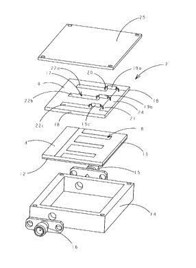
In Figure 1, there is shown a switch 2 according to the preferred
embodiment of the present invention,. The switch 2 consists of two layers 4
to and 6. The layer 4 consists of a first HTS microwave circuit 8 printed on a
substrate 10 attached to a ground plane 12. The HTS circuit 8 is assembled
in a housing 14 by epoxying the ground plane 12 to the bottom of the housing
14. The input/output 15 and 16 are attached to the HTS circuit 8. Layer 6
consists of a second microwave circuit 17 printed on a substrate 18.
Preferably, there is no ground plane immediately beneath the substrate 18. if
desired, a ground plane could be located beneath the substrate 18 with
openings where required for coupling purposes. The layer 6 is placed on the
top of the layer 4 by using low loss adhesive or any other means. The layer 6
can be spaced apart from the layer 4 by supports (not shown) leaving an air
2o space between the two layers. The circuit is assembled with three on/off
switch elements 19a, 19b and 19c. Each switch element has two terminals 20,
21. One terminal 20 is connected to the circuit 17 and the other terminal 21
is connected to a transverse line 24 which is short-circuited to the housing
14.
4
CA 02251517 1999-OS-21
A plate 25 is a top cover for the switch 2. There is one switch element for
each transmission line of the circuit 17.
Figure 2 illustrates a detailed description of the HTS circuit 8. Each of
the transmission lines 26a, 26b and 26c represent one port of a T junction.
The three T junctions are connected by HTS transmission lines. The number
of sections (T junctions) determines the bandwidth of the switch. The more
sections the circuit has, the wider the bandwidth the switch would exhibit.
Thus, a switch can have more than three or fewer than three T junctions. The
circuit has two contact pads 28a, 28b made out of gold or any other metals to
to allow connections to the input and output connectors.
Figure 3 illustrates a detailed description of the circuit 17 printed on
the layer 6- It consists of three transmission lines 22a, 22b and 22c mounted
on the substrate such that the centre of the lines 22a, 22b and 22c align with
transmission lines 26a, 26b and 26c (not shown in Figure 3) respectively
shown in Figure 2. The widths and the lengths of the lines 22a, 22b and 22c
do not have to be necessarily the same as the widths and lengths of the lines
26a, 26b and 26c respectively. The lines 26a, 26b and 26c are coupled either
capacitatively or inductively to the lines 22a, 22b and 22c respectively. The
transmission lines 22a, 22b and 22c are made out of HTS, gold or any other
2o metals. Three switch elements 19a, 19b and 19c are connected to the circuit
17. The switch elements can be PIN, FET or GaAs diodes. One terminal 20
of'each switch element 19a, 19b and 19c is connected to the ends of the
transmission lines 22a, 22b and 22c respectively. The other terminal 21 of
each switch element 19a, 19b and 19c is connected to the transverse line 24,
5
CA 02251517 1999-OS-21
which is short-circuited to the housing. Mechanical type switches could be
used
instead of diodes to short circuit the gap between the lines 22a, 22b 22c and
the
transverse line 24. Alternatively MEMS ( Micro-Electro-Mechanical System)
switches could be used for the switch elements 19a, 19b and 19c or mechanical
switches could be used. The switch elements are synchronously turned on/off.
The
switch shown in Figure 1 is in the ON state when the switch elements are in
the ON
state and the switch circuit is in the OFF state when the switch elements are
in the
OFF state. Thus, the operation of the switch is controlled by the ON/OFF
positions
of the switch elements. The switch could be designed to operate in an opposite
manner where the switch circuit is ON when the switch elements are OFF and
vice
versa.
In Figure 4, there is a shown a further embodiment for a circuit 30 of the
second layer 6. The same reference numerals are used for those components that
are
the same as the components of Figure 3. The lines 22a, 22b and 22c are made
out of
HTS material. The switch elements are narrow transmission lines 32a, 32b and
32c,
which are also made out of HTS material. DC current is supplied to the lines
32a,
32b and 32c through inductors 34a, 34b and 34c respectively connected to
conductors 35a, 35b and 35c respectively. When the DC current is off, the
lines 32a,
32b and 32c are superconductive and a short circuit exists through the
transverse line
24 of the layer 6. The switch 2 is then in the ON position and the switch
elements
are also in the ON position. When the DC current is switched on and is high
enough,
the narrow transmission lines 32a, 32b and 32c switch from the superconductive
state to the non-superconductive state. The switch elements are then in the
off position and the switch 2 is in the off position.
6
CA 02251517 1998-11-13
By the two layer arrangement disclosed, the RF and DC signals are isolated
from one another.
In Figure 5, there is shown a further embodiment of a circuit 36 on
the layer 6. T'he same reference numerals are used in Figure 5 as those used
5 in Figure 3 for those components that are identical. The circuit 36 and the
transverse line 24 are laid out in a manner similar to that shown in Figure 3
for the circuit 17 and the transverse line 24 on the substrate 18 except that
the
two circuits 36, 24 are interconnected using flip-chip technology. The
transmission lines (22a, 22b and 22c - of which only 22a is shown in Figure
to 5) which make up the circuit 36 as well as the transverse line 24 are made
from metal that is compatible with flip-chip technology. Substrate 18 is also
made of a material that is compatible with flip-chip technology. A chip 37,
supported by chip bumps 38 is connected between the transmission line 22a
and the transverse line 24. A chip and chip bumps will also connect the
15 transmission lines 22b (not shown) to the transverse line 24 and a further
chip and chip bumps will connect the transmission line 22c (not shown) to
the transverse line 24 even though only one chip 37 is shown in Figure 5.
The chip 37 can be a PIN or FET diode, which is connected to a DC power
supply (not shown). The DC power supply switches the chip on and off,
2o thereby causing the switch 2 to turn on and off respectively. The flux
which
is typically generated during the soldering process of the chip bumps can
damage HTS material. The two layer circuit where the bottom layer 4 uses
HTS material as shown in Figure 2 while the top layer 6 employs the flip-
chip technology allows the combination of flip-chip technology with HTS
CA 02251517 1998-11-13
technology as the layer 6 can be manufactured separately from the layer 4.
The diode shown in Figure 5 is in chip form. Alternatively, the diode could
be in encapsulated form (not shown) where the diode is attached between the
line 22a and the transverse line 24 using wire bonding or other suitable
5 means. The configuration of the layer 6 shown in Figure 5 still permits the
isolation between IRF and DC signals.
In Figure 6, there is shown yet another embodiment of a circuit 39 on
the layer 6. The same reference numerals are used in Figure 6 for those
components that are identical to the components of Figure 3. As with Figure
l0 5, only one transmission line 22a is shown, but the transmission lines 22b
and 22c are laid out in a manner similar to that shown in Figure 3. As can be
seen, a microelectromechanical (MEMS) system 40 connects the
transmission line 22a of the circuit 39 with the transverse line 24. Second
and third MEMS switches (not shown) would connect transmission lines 22b
15 and 22c (also not shown) to the transverse line 24. The MEMS switches are
placed on the substrate 18 to interconnect the circuits 39 with transverse
line
24 using conventional MEMS technology. MEMS technology is not directly
compatible with HTS technology but the layer 6 can be manufactured using
conventional MEMS technology separate and apart from the layer 4, which
2o can use HTS technology. After manufacture, the two layers can be brought
together.
The three embodiments of the layers 6 shown in Figures 4, 5 and 6
respectively can be substituted for the embodiment shown in Figure 3 of the
layer 6 and placed into the switch 2 of Figure 1. While the embodiment
CA 02251517 1998-11-13
shown in Figure 6 is the preferred embodiment, there may be circumstances
requiring particular performance characteristics where one of the other
embodiments will be preferred.
Figure 7 shows a preferred embodiment for a C-switch 42. An HTS
5 switch 42 consists of two layers 4 and 6. Layer 4 consists of an HTS circuit
44 having four ports 46a, 46b, 46c and 46d printed on a substrate 10 attached
to a ground plane 12. The layer 6 has a circuit 48 consisting of several
transmission lines SOa, SOb, SOc, SOd, SOe, SOf, SOg, SOh mounted on a
substrate 18 to align with the lines 47a, 47b, 47c, 47d, 47e, 47f, 47g, 47h
10 respectively of the layer 4. The circuit 44 is assembled in a housing by
attaching the ground plane 12 to a bottom of the housing 52 using epoxy
soldering or any other means. A bottom side of the layer 6 is attached to the
top side of the layer 4 using adhesive or any other suitable means. The
switch elements (not shown) could be of the semiconductor type or
15 mechanical type. Each switching element has two terminals. One terminal is
attached to the lines SOa-SOh while the other terminal is attached to circuits
60a, 60b, 60c and 60d, which are short circuited to the housing 52. The plate
25 is used as a cover for the circuits shown.
Figures 8a and 8b show the measured results for an HTS C-switch 42
20 as described in Figure 7. The graph shown in Figure 8a is a graph of the
isolation and return loss when the switch is on and the graph shown in Figure
8b is a graph of the isolation and return loss when the switch is off. The
switching elements used in the switch 42 for the measured results shown are
the narrow HTS line switching elements shown in Figure 4.
9
CA 02251517 1998-11-13
In Figure 9, there is shown a single layer switch 61 having a circuit
62 on a layer 64 of a substrate 65. The switch elements are narrow HTS lines
66a, 66b and 66c driven by DC current in the same manner as those shown in
Figure 4, but not shown in detail in Figure 9. Capacitors 68a, 68b and 68c
5 are located at the end of each of the three transmission lines 69a, 69b and
69c. Conductors 34a, 34b and 34c extend from conductors 35. The circuit
62 is mounted in a housing 70 having an input 72 and output 74 with a cover
76. Isolation between RF and DC is achieved by the capacitors 68a, 68b and
68c. The layer 64 is bonded into the housing 70 by epoxy (not shown).
to Figures l0a and l Ob shown the measured results of the switch 61 of Figure
9.
It can be seen that Figure l0a is a graph of the isolation and return loss
when
the switch is on and Figure lOb is a graph of the isolation and return loss
when the switch is off.
The present invention can be used to construct different types of
15 switches including single pole double throw switches and with various
switch matrices. While >=iTS switches are the preferred embodiment, the
lower layer in a two layer switch can be made with a gold film on the
substrate in place of the HTS film. Similarly, the transmission lines
extending between an input and output can be made from I-STS film, gold
2o film or other suitable metallic film. The number of transmission lines and
switch elements will vary with the bandwidth desired. While the present
invention has been described as a switch and that is the preferred
embodiment, the two layer embodiment can be used to interact with and
control microwave circuits. Further, the present invention can be used to
10
CA 02251517 1998-11-13
construct H'TS microwave circuits using two layers to combine technologies
that are incompatible with HTS into the HTS circuit. This is accomplished
by dividing the circuit into two layers and constructing part of the circuit
on
the first layer and part of the circuit on the second layer.
Although the present invention has been fully described by way of
example in connection with a preferred embodiment thereof, it should be
noted that various changes and modifications will be apparent to those
skilled in the art. Therefore unless otherwise such changes and modifications
depart from the scope of the present invention, they should be construed as
1 o being included therein.
11