Note : Les descriptions sont présentées dans la langue officielle dans laquelle elles ont été soumises.
Docket no.: 12622-004
Title of the Invention
Compact polarized omnidirectional helical antenna
[001] Field of the Invention
[002] The present invention relates generally to radio frequency (RF)
electromagnetic signal
broadcasting systems. More particularly, the present invention relates to
circularly polarized
omnidirectional helical antenna for unmanned vehicle telemetry and/or video
broadcasting or
other applications where weight and/or space are of concern.
Background of the Invention
[003] Circular polarized antennas have been adopted by UAV/UAS hobbyists and
professionals
for their multi-path rejection properties and their immunity to polarization
losses. However, the
commonly used circular polarized designs are relatively big versus their
linear counterpart and
fragile when made light enough for aircraft purpose.
[004] Newly adopted rules also limit the weight of unmanned aircraft and have
pushed forward
the appearance of ever smaller/lighter aircraft. Even at frequency of 5.8GHz,
circularly polarized
antennas often are a substantial part of the vehicle. The common designs
consist of multiples
wires or thin metal sheets bent in lobes, assembled in a floral like shape
(See Figure 11A). Such
designs are costly to fabricate and have tolerances errors.
[005] There is thus a need for new circular polarized antennas particularly
adapted to unmanned
vehicle telemetry, such as drones and/or video broadcasting or other
applications where weight
.. and/or space is a concern.
Summary of the Invention
[006] The shortcomings of the prior art may be generally mitigated by a
compact circular
polarized omnidirectional helical antenna providing smaller and lighter
circular polarized
antennas.
1
CA 2968566 2019-07-16
Docket no.: 12622-004
[007] A compact polarized omnidirectional helical antenna is described herein.
The antenna
may be fabricated from lightweight printed circuit board (PCB). Using the PCBs
in fabrication of
the antenna may be cheaper and have higher predictability, thus leading to
smaller fabrication
errors compared to the antennas made with wires.
[008] In accordance with at least one embodiment, there is provided an antenna
comprising: at
least one antenna bay comprising an input port; a feed network, the feed
network comprising a
center node connected to the input port; a printed circuit board (PCB)
comprising: an active
surface comprising at least two feed micro-strips; a reference surface
comprising at least two
reference micro-strips, the reference surface being opposite to the active
surface; a radiative
component, the radiative component comprising: at least two dipoles, each of
the at least two
dipoles being shaped as a helix and being uniformly disposed about an axis of
the antenna, each
of the at least two dipoles comprising: a dipole feed portion connected to one
of the at least two
feed micro-strips; a dipole reference portion connected to one of the at least
two reference micro-
strips.
[009] The at least two dipoles may be equidistant from the antenna axis. All
of the at least two
feed micro-strips may have an equal length. All of the at least two reference
micro-strips may
have an equal length.
[0010] The antenna may further comprise at least two dipole feed nodes at the
operative
connection of the feed micro-strips and the dipole, each of the dipole feed
nodes being proximal
to an edge of the first PCB, the at least two dipole feed nodes being
uniformly distributed along
the edge of the first PCB.
[0011] The antenna may further comprise at least two dipole reference nodes at
the operative
connection of the reference micro-strips and the dipole, each of the at least
two dipole reference
nodes being proximal to the edge of the first PCB, the dipole reference nodes
being uniformly
distributed along the second circumference.
[0012] The at least two dipole feed nodes may be on a first circumference of
the PCB and the at
least two dipole reference nodes may be on a second circumference of the PCB.
The diameter of
the first circumference may be equal to the diameter of the second
circumference.
2
CA 2968566 2019-07-16
Docket no.: 12622-004
[0013] The shape of the reference micro-strip may be the same as the shape of
the feed micro-
strip.
[0014] The width of the feed micro-strip may be larger at the feed node than
at the center node
and the width of at least some of the reference micro-strip being narrower at
the reference node
than at the center node.
[0015] The width of each reference micro-strip at the reference node may be
approximately equal
to the width of the feed micro-strip at the feed node.
[0016] The antenna may further comprise a plurality of second reference micro-
strips located on
the reference surface, each second reference micro-strip connecting the
central node to each of
the plurality of dipole feed nodes, each of the second reference micro-strip
mirroring one of the
first reference micro-strip.
[0017] At least some of the reference micro-strips may be parallel to one of
the plurality of feed
micro-strips.
[0018] Each of the second reference micro-strip may be symmetric relative to
an axis stretching
between the reference port and one of the reference nodes.
[0019] The at least two dipoles may be printed on a second PCB, the second PCB
being flexible
and adapted to form a helical conformation of the at least two dipoles.
[0020] In at least one embodiment, the antenna may further comprise a second
antenna bay,
wherein each antenna bays are oriented on the antenna axis and wherein
reference nodes of
corresponding dipoles in the first and the second antenna bays are aligned
with reference to the
antenna axis.
[0021] The antenna may further comprise a radome enclosing at least a portion
of the antenna.
[0022] The dielectric constant of the first PCB may be at least 4.
[0023] In at least one embodiment, the input port may comprise an inner
conductor and an outer
conductor.
[0024] In accordance with another embodiment, there is provided an antenna
comprising an
antenna bay, the antenna bay comprising: a primary radiator, a plurality of
parasitic dipoles, each
3
CA 2968566 2019-07-16
Docket no.: 12622-004
of the parasitic dipoles being shaped as a helix with reference to the primary
radiator axis.
[0025] The plurality of parasitic dipoles may be uniformly distributed with
azimuth about an axis
of the primary radiator.
[0026] The primary radiator may be a dipole. The primary radiator may be a
monopole antenna.
[0027] The antenna may further comprise a dipole with operatives to prevent
transmission lines
induced imbalance (balun).
[0028] The parasitic dipoles may be printed on a flexible PCB, the flexible
PCB being
deformable as a helical conformation of the respective parasitic dipoles
thereof.
[0029] The antenna may further comprise a radome at least partially enclosing
the antenna.
[0030] The helical parasitic dipoles may be arranged as to convert linear
radiations from a pre-
existing linear polarized dipole or monopole antenna into substantially
circular polarized
radiations.
[0031] The parasitic dipoles may further comprise operatives to hold, maintain
or fix a pre-
existing dipole or monopole antenna substantially at its center.
.. [0032] In accordance with another embodiment, a printed circuit board (PCB)
for an antenna is
provided. The PCB includes an active surface having one or more feed micro-
strips; and a
reference surface having a plurality of reference micro-strips, the reference
surface being
opposite to the active surface, wherein the feed micro-strips and the
reference micro-strips are
operatively connected to a plurality of dipoles, each of the dipoles being
shaped as a helix and
being uniformly disposed about an antenna axis.
[0033] The antenna axis may be the central axis of the antenna, the PCB may
comprise a center
node connected to the feed micro-strips and the reference micro-strips.
[0034] All of the plurality of the feed micro-strips and the reference micro-
strips may have the
same length.
[0035] Each feed micro-strip may be tapered, being narrower at the center
node; and each
reference micro-strip may be tapered, being wider at the center node.
[0036] The PCB may further comprise a plurality of second reference micro-
strips located on the
4
CA 2968566 2019-07-16
Docket no.: 12622-004
reference surface, the second reference micro-strips connecting the reference
node to each of the
plurality of dipole reference nodes, the second reference micro-strip
mirroring one of the first
reference micro-strip and being symmetric relative to an axis stretching
between the reference
port and one of the reference nodes.
[0037] In accordance with another embodiment, a radiative component for an
antenna is
provided. The radiative component for the antenna includes at least two
dipoles, each of the two
dipoles being dipole micro-strips located on a substrate, so that when the
substrate is deformed,
the at least two dipoles are shaped as a helix and uniformly disposed about an
antenna axis. The
at least two dipoles may comprise: a dipole feed portion configured to be
connected to one of a
.. plurality of feed micro-strips and a dipole reference portion configured to
be connected to at least
one of the reference micro-strips.
[0038] Advantageously, the antenna according to the present invention may
occupy
approximately 20% of the volume of the commonly used designs.
[0039] The antenna as described herein may be used for broadcasting radio
frequency
electromagnetic signal.
[0040] Other and further aspects and advantages of the present invention will
be obvious upon an
understanding of the illustrative embodiments about to be described or will be
indicated in the
appended claims, and various advantages not referred to herein will occur to
one skilled in the art
upon employment of the invention in practice.
Description of the Drawings:
[0041] The above and other aspects, features and advantages of the invention
will become more
readily apparent from the following description, reference being made to the
accompanying
drawings in which:
[0042] Figure 1 is a perspective top view of an embodiment of the antenna
according to the
principles of the present invention.
5
CA 2968566 2019-07-16
Docket no.: 12622-004
[0043] Figure 2 is the top view of a micro-strips network (active surface) on
a first PCB
according to a preferred embodiment of the present invention.
[0044] Figure 3A is the bottom view of the micro-strips network (reference
surface) on the first
PCB according to the principles of the present invention.
[0045] Figure 3B is the bottom view of the micro-strips network (reference
surface) on the first
PCB according to the principles of the present invention.
[0046] Figure 3C is a top see-through view of an example embodiment of the
micro-strips
network with tapered micro-strips.
[0047] Figure 4 is a side view of the dipoles traced on a first radiative
component in its flat state
according to a preferred embodiment of the present invention.
[0048] Figure 5 is a perspective view of the first radiative component in
accordance with the
principles of the present invention.
[0049] Figure 6 is a perspective top view of the network attached to a common
coax cable with
connector according to the principles of the present invention.
[0050] Figure 7 is a perspective bottom view of the network with common coax
cable according
the principles of the present invention.
[0051] Figure 8 is a perspective top view of an embodiment of the antenna
according to the
principles of the present invention.
[0052] Figure 9 is a side view of the dipoles traced on a second radiative
component in its flat
state according to the principles of the present invention.
[0053] Figure 10 is a perspective view of the second radiative component
according to the
principles of the present invention.
[0054] Figure 11A is a perspective view of a prior art antenna.
6
CA 2968566 2019-07-16
Docket no.: 12622-004
[0055] Figure 11B is a perspective view of the antenna in accordance with the
principles of the
present invention.
Detailed Description of the Preferred Embodiment
[0056] A novel compact polarized omnidirectional helical antenna will be
described hereinafter.
Although the invention is described in terms of specific illustrative
embodiments, it is to be
understood that the embodiments described herein are by way of example only
and that the scope
of the invention is not intended to be limited thereby.
[0057] Helix shape (26 at Fig. 1) as used herein generally means helix or
almost helix shape
about an axis specified herein, i.e. having a constant or approximately
constant angle with the
.. axis specified herein.
[0058] A single-feed circularly polarized omnidirectional helical antenna is
disclosed herein. Due
to the implementation as described herein, the antenna may be both compact and
lightweight.
Such antenna may be used for unmanned aircrafts, such as drones, for unmanned
vehicle
telemetry and/or video broadcasting. The antenna may also be used in other
applications where
weight and/or space of the antenna are of concern.
[0059] Advantageously, the antenna fabricated according to the present
invention may occupy
approximately 20% of the volume of the commonly used designs.
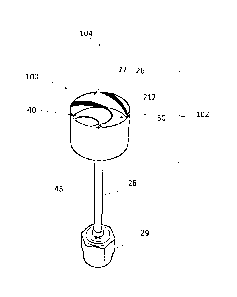
[0060] Referring now to Fig. 1, an antenna 100 according to a preferred
embodiment of the
present invention is shown. The antenna 100 comprises at least one antenna bay
102. Each
.. antenna bay 102 comprises a feed network 50 and a first radiative component
27. The feed
network 50 generally comprises micro-strips 40. The first radiative component
27 typically
comprises at least two dipoles 26. In a preferred embodiment, the feed network
50 is operatively
connected to the first radiative component 27 at a junction 212.
[0061] The antenna 100 further comprises an input port 43. In a preferred
embodiment, the input
.. port 43 is coaxial input port having an inner conductor and an outer
conductor (not shown at
Figures). The outer conductor may serve as a reference potential.
7
CA 2968566 2019-07-16
Docket no.: 12622-004
[0062] Still referring to Figure 1, the antenna 100 is adapted to be connected
to cable 28. In a
preferred embodiment, the cable 28 is typical coax cable 28 connected to a SMA
(Sub Miniature
version A) connector 29. Understandably, any known mean or connector for
connecting the
antenna 100 may be used without departing from the principles of the present
invention.
[0063] In at least one embodiment, a lightweight printed circuit board (PCB)
may be used for
manufacturing the antenna bay 102. The antenna bay 102 generally comprises a
power
distribution and matching network 50. In a preferred embodiment, the matching
network 50 may
be located on a generally circular PCB comprising a micro-strips manifold, an
input port and at
least two micro-strip arms (also referred herein as "micro-strip").
[0064] In a preferred embodiment, the antenna 100 comprises one or more bays
102 of helical
dipole radiators 26. The helical dipole radiators 26 are generally excited
using a manifold of
micro-strips as feeding/matching network 50. Alternatively, the bay 202 of
helical dipoles 226
may be used as parasitic radiator of a common dipole antenna 233, effectively
converting the
common dipole antenna 233 into a circularly polarized omnidirectional helical
antenna 200, as
shown at Fig. 8.
[0065] Referring again to Fig. 1, in at least one embodiment, the power
distribution and matching
network (together referred to herein as "feed network 50" or "micro-strips
network 50") may
consist of a generally circular or round PCB 21 comprising micro-strips
(manifold), an input port
and at least two micro-strip arms 40. At the end of each micro-strip arm 40,
helical dipoles 26
may be axially wound in reference to the axis 104 of the antenna 100.
[0066] In a preferred embodiment, the length of each micro-strip arm 40 is 90
electrical degrees.
[0067] As an example, the antenna 100 may comprise four dipoles 26, each
dipole 26 having a
helical orientation and having an approximate fourfold rotational symmetry
with reference to a
common antenna axis 104.
[0068] Now referring to Fig. 2, an embodiment of a PCB 21 comprising a micro-
strips network
50 is shown. In such an embodiment, the first PCB 21 comprises an active plane
22 (also called
herein as an "active surface") of the micro-strips network 50. The active
plane 22 is shaped in
8
CA 2968566 2019-07-16
Docket no.: 12622-004
order to achieve the desired length within dipoles arrangement. In at least
one embodiment, a
central node 23 is connected to the input port 43.
[0069] Now referring to Figure 3A, the bottom surface of an exemplary PCB 21
comprising a
reference plane 24a (also called herein as "reference surface" of PCB) of the
micro-strips
network 50 is shown. In such an exemplary PCB 21, the micro-strips network 50
is shaped as two
generally "S" shape crossing about their center.
[0070] Now referring to Figure 3B. another exemplary embodiment of a micro-
strips network 50
being shaped as two generally "S" shape crossing about their center and two
generally inverted
"S" shape crossing about their center. Understandably, any other design having
micro-strips
allowing a connection with the periphery may be used without departing from
the principles of
the present invention.
[0071] In at least one embodiment, the micro-strips 40, 47 and 48 on Fig. 3A
and 3B may have a
form of an arc or any other form of detour in order to accommodate the
electrical length needed
for matching of the dipoles to the feed line within the space between the
dipoles.
[0072] Still referring to Figure 3B, in some embodiments, the bottom
(reference) micro-strip 47
on the reference surface 24b may be doubled by doubling micro-strips 49 (also
referred herein as
"second reference micro-strips") to be substantially symmetric in regard to an
axis drawn
between the dipole feed nodes 48 and the reference port 45. Each second
reference micro-strip 49
may connect the central node 45 to each of the plurality of dipole feed nodes
48, each of the
second reference micro-strip 49 mirroring one of the first reference micro-
strip 47 and being
symmetric relative to the axis stretching between the reference port 45 and
one of the reference
nodes 48.
[0073] Preferably, the width of the micro-strips 40, 47 and 48 may be adjusted
following the
rules of the art. As an example, the width of the micro-strips 40, 47 and 48
may be adjusted in
order to achieve proper impedance match from the helical dipoles 26 (see
Figures 4 and 5) to the
feed line 28.
9
CA 2968566 2019-07-16
Docket no.: 12622-004
[0074] In at least one embodiment, the reference plane 24a, 24b of the micro-
strip network 50
may be substantially symmetric and/or tapering into a parallel strip. In a
preferred embodiment,
at the reference port 45, the reference micro-strips 47, 49 is about three
times wider than the feed
micro-strips 40, while at the feed nodes 25, the width of the feed micro-strip
40 and the width of
the reference micro-strips 47, 49 are about the same.
[0075] In yet another embodiment, the micro-strips 40 may have double tapered
shape. The
double tapered shape generally aims at providing a smooth transition between
the unbalanced
coax feed line 28 and the balanced helical dipoles feed 33. The double tapered
shape may consist
of gradually widening the top (active) trace (also referred herein as "feed
micro-strip") and a
gradually narrowing bottom (reference) trace (also referred herein as
"reference micro-strip"). In
such an embodiment, when the reference micro-strips 47, 49 are wider, the feed
micro-strips 40
are narrower. Such configuration generally aims at conserving the impedance
relatively constant
throughout the length of the micro-strips.
[0076] As an example, each feed micro-strip 40 may be tapered, as shown at
Fig. 2. In such an
embodiment, the width of the micro-strip 40 is generally larger about the feed
node 25 compared
to the center node 23.
[0077] The micro-strip 47 of the reference surface may also be tapered.
Referring to Figs. 3A and
3B, the width of the tapered micro-strip 47 it is smaller at the reference
node 48 compared with
the width of the micro-strip 47 at the reference port 45. The width of each
tapered reference
micro-strip 47 at the reference node 48 are approximately equal to the width
of the feed micro-
strip at the feed node 25. In such an embodiment, the width of the top and
bottom trace (micro-
strips 40, 47, 49) may be generally equal at the feed point 25 of the dipole.
Being equal, the
micro-strips 40, 47, 49 become a substantially parallel strips balanced
transmission line.
Referring now to Fig. 3C, shown therein is a see-through view of such example
embodiment of
the feed network 50 comprising tapered micro-strips 40, 47, 49. While the feed
micro-strips are
located on the feed surface 22, the reference micro-strips 47, 49 are located
on the reference
surface. Tapering of the micro-strips 40, 47, 49 relevant to each other are
shown.
[0078] One of the advantages of such arrangement is that the unbalanced
current flowing on the
CA 2968566 2019-07-16
Docket no.: 12622-004
outside of a coaxial transmission line are minimized, safeguarding the
antenna's circular
properties.
[0079] In a preferred embodiment, the micro-strips 40 may have an impedance
adjusted to match
the impedance of the dipoles 26 (for example, four dipoles) to the feed line
28 (shown. for
example, at Figure 1 described herein). In a typical embodiment, the input
port preferably
consists of a hole or aperture 23 in a first PCB 21 that may permit soldering
of the conducting
cable or connector, such as a center portion of a coaxial cable to the active
plane 22.
[0080] In at least one embodiment, at least two dipole feed nodes 25 are
located at the operative
connection 212 of the feed micro-strips 40 to the dipole 26. On yet another
embodiment, the
dipole feed nodes 25 are located on a same circumference (also referred herein
as first or feed
circumference) and the at least two dipole feed nodes 25 are uniformly
distributed along the first
circumference. Such first circumference is preferably proximal to an edge of
the first PCB 21.
[0081] In at least one embodiment, at least two dipole reference nodes 48 are
located at the
operative connection of the first reference micro-strips 47 to the dipole 26.
In yet another
embodiment, each of the at least two of dipole reference nodes 48 are located
on the same
circumference (also referred herein as second or reference circumference). The
dipole reference
nodes 48 are uniformly distributed along the second circumference. Such second
circumference is
preferably proximal to an edge of the first PCB 21.
[0082] In a preferred embodiment, the PCB 21 is shaped to allow the feed nodes
25 to be located
on the first circumference and to allow the reference nodes 48 to be located
on the second
circumference. In a preferred embodiment, the first and the second
circumferences have an equal
radius. In least one embodiment, the first radiative component 27 may be
printed on a flexible
PCB. In such an embodiment, the shape of the first radiative component 27 is
generally
deformed. The deformed shaped is, in a preferred embodiment, a helical
conformation of the
dipoles 26. In a preferred embodiment, the dipoles 26 are generally shaped as
a rectangular sheet
of flexible PCB. The dipoles 26 are wound in a generally cylindrical shape
around the matching
network 50 for an entire PCB material construction. Wounded flexible dipoles
26 are generally
=
11
CA 2968566 2019-07-16
Docket no.: 12622-004
suitable for mass production. Understandably, other shapes and configuration
may be used
without departing from the principles of the present invention.
[0083] Now referring to Fig. 4, an exemplary embodiment of a first radiative
component 27 is
shown as implemented on a second PCB 327. As an example, referring to Figure
4, the first
radiative component 27 is shown unfolded. Now referring to Figure 5, the first
radiative
component 27 is folded at one side to connect to another side to form a
generally cylindrical
shape.
[0084] In some embodiments, the first radiative component 27 is made of any
flexible material
adapted to receive dipoles 26, such as PCB material or any other material
comprising dipoles 26.
In a preferred embodiment, the material used for substrate 327 of the first
radiative component 27
is polyimide. The substrate 327 of the first radiative component 27 may also
be made of any
other type of flexible material adapted to be rolled or folded as a cylinder.
For example, the
substrate 327 may be made of plastic, glass fiber, Polytetrafluoroethylene,
e.g. Teflon.
[0085] Now referring to Figure 4, the first radiative component 27 may
comprise printed dipoles
26 (also referred herein as "dipole elements"). In some embodiments, each of
the dipoles 26
comprises a feed portion 37 and a reference portion 39. The feed portion 37
and the reference
portion 39 are separated with a gap 31. The gap is generally defined by a
reference node 35 and
feed node 33. For example, the gap 31 may be approximately the same width as
the width of the
first PCB 21 (e.g. distance between a feed surface and a reference surface).
[0086] Still referring to Figure 4, in a preferred embodiment, the angle a is
within a range of
about 17 to about 23 . The angle a may generally vary based on the diameter
of the feeding PCB
21. For example, if the diameter of the PCB is 214, the angle a may be 22.5 ,
where A, is the
wavelength. For example, if diameter of the PCB is 212, the angle a may be 45
, if diameter of
the PCB is 2/8, the angle a may be 11 .
[0087] In yet another embodiment, the first PCB 21 has a dielectric constant
of more than 3. In
some other embodiments, the first PCB 21 may have a dielectric constant of 4
or more.
Preferably, the first PCB 21 has a dielectric constant of about 4.5.
12
CA 2968566 2019-07-16
Docket no.: 12622-004
[0088] In a preferred embodiment, the first radiative component 27 is flexible
enough to be rolled
as a cylinder shape. Referring to Fig. 5, an example embodiment of the first
radiative component
27 being rolled in a cylinder shape is shown. In at least one embodiment, the
internal diameter of
such cylinder may be substantially equal to the diameter of the matching
network 50 of the first
PCB 21.
[0089] In a preferred embodiment, the internal diameter of the rolled cylinder
of the first
radiative component 27 is adapted to receive the first PCB 21. The first
radiative component 27,
when rolled in a cylindrical shape, may be adapted to receive the dipoles
elements 26 in their
rolled form. In a preferred embodiment, the dipole elements 26 are rolled in a
way to face the
interior of the cylinder.
[0090] Now referring to Fig. 6, an embodiment of an antenna 100 shown without
the radiative
component 27 is presented. The matching network 50 is installed on a common
coax cable 28
comprising a SMA (Sub Miniature version A) connector 29. The center 210 of the
surface is
adapted to receive the center portion of the coaxial cable 28 to create a
connection with the
network 50. The inner portion of the coaxial cable 28 may be soldered or
welded to the active
plane 22 to provide an electric connection.
[0091] Now referring to Fig. 7, an embodiment of the antenna 100 without the
radiative
component 27 is shown. The outer portion of the coax cable 28 is preferably
attached to the
reference surface 24b. The attachment 211 may be any type of attachment mean
known in the art,
such as soldering or welding.
[0092] Referring now to Figures 1-7, in a preferred embodiment, the feed
points 33, 35 of the
dipole 27 may connect to the bottom and top traces 40, 47, 49 of the network
50 on the edge 51
of the first PCB 21. The connection of the feed points 33, 35 to the network
50 may be a solder
joint or a weld joint to connect the junction 212 to the micro-strips 40 and
the dipoles elements
26.
[0093] Now referring to Fig. 8, a further embodiment of the antenna 200 is
shown. In such an
embodiment, the antenna 200 comprises a second radiative component 227 and a
bushing 215.
13
CA 2968566 2019-07-16
Docket no.: 12622-004
The bushing 215 may be made of plastic or any non-conductible material, such
as non-metallic
material. The bushing 215 generally aims at attaching the primary dipole
radiator 233 to the
surface of the second radiative component 227, preferably being attached
within the center of the
cylindrical radiator 227. The second radiative component 227 may be made of a
PCB.
[0094] The antenna 200 further comprises a set of helical shaped dipoles 226.
The helical shaped
dipoles 226 are preferably shorted in single continuous conductors, thus
aiming at being
substantially parasitic radiating elements. In a preferred embodiment, the
continuous conductors
may be placed around a common dipole 233 or a monopole primary radiator.
[0095] The antenna 200 aims at limiting the use of parallel-strips network but
having a taller
dipole primary radiator 227. In such an embodiment, the primary radiator may
be a common
sleeve dipole 216 or any other purely linear omni-directional radiator using
any method to limit
coax imbalance current.
[0096] The helical shaped parasitic dipoles arrangement may also be used as
singular unit to
retrofit existing common dipole antennas, converting them from substantially
linear radiation
mode to substantially circular radiation mode.
[0097] Referring now to Fig. 9, an alternate embodiment of a flexible strip
227 comprising a
plurality of parasitic dipoles 226 to be rolled into the radiator is shown.
The flexible strip 227
may be made of PCB.
[0098] Now referring to Fig. 10, in a preferred embodiment, the flexible strip
227 is made of
flexible material and may be shaped as to be rolled or folded as a cylinder.
In at least one
embodiment, the internal diameter of the formed cylinder may be substantially
equal to the
diameter needed to provide circular polarisation. The antenna 200 may have a
similar layout of
the helical dipoles 226 as antenna 100, but with indirect feeding of the
dipoles 226 from a
centrally placed dipole 233 or monopole antenna. It should be noted that such
an embodiment
allows that the circular polarization direction of antenna 200 be reversed
from the antenna 100
due to the 180-degree delay created by the parasitic elements.
14
CA 2968566 2019-07-16
Docket no.: 12622-004
[0099] The radiative component 227 may be made of any flexible material
allowing dipoles 226,
such as PCB material. In a preferred embodiment, the material used for
substrate 427 of the
radiative component 227 is polyimide. The substrate 427 of the flexible strip
227 may also be
made of any other material flexible enough to be rolled into a cylinder. For
example, the substrate
427 may be made of plastic, glass fiber, Polytetrafluoroethylene, e.g. Teflon.
[00100] Still referring to Fig. 10, the flexible strip 227 formed as a
cylindrical shape
comprising the parasitic dipoles elements 226 in their rolled form is shown.
[00101] Once formed, the antenna 100, 200 may be placed in a molded
plastic, a radome or
other durable and RF transparent material, generally aiming at increasing
protection of the
antenna 100, 200.
[00102] In accordance with another embodiment, the antenna 100, 200 may
further
comprise a second antenna bay 102, 202. The first and the second antenna bays
102, 202 may be
oriented on a common antenna axis 104, wherein radiative components of the
respective antenna
bays 102, 202 may be substantially identical in structure. The reference nodes
of corresponding
dipoles 26, 226 in respective antenna bays 102, 202 may be aligned with
reference to the antenna
axis 104.
[00103] The antenna 100, 200 may further comprises a radome (not
shown). The radome
may enclose the other components of antenna 100, 200 at least partially for
protecting the
antenna 100. 200.
[00104] The antenna 100, 200 may be used for broadcasting radio frequency
electromagnetic signal. In a preferred embodiment, the antenna 100, 200 is a
single-feed
circularly polarized omnidirectional helical antenna. The broadcasting of
radio frequency
electromagnetic signal may be used by, but not limited to, unmanned vehicle
telemetry (such as
drone) and/or video broadcasting or other applications where weight and/or
space is of concern.
[00105] Now referring to Fig. 11, a preferred embodiment of the present
invention 214 is
shown aside with an exemplary prior art 213 antenna. Typically, the prior art
antennas 213
occupy a volume of a demi-sphere having a radius of 1/4 X, where X (lambda) is
the wavelength.
CA 2968566 2019-07-16
Docket no.: 12622-004
For example, if X, is 23 cm for a demi-sphere, the value of CA * k) provides
radius (r) of 5.75 cm.
As the volume of a sphere having a radius of 5.75 cm is about 800 cm2 (the
volume of a sphere
being 4/3*er), the volume of a demi-sphere of a typical prior art antenna 213
is 400 cm2.
Advantageously, the antenna 100 as described herein may take about 20% of
volume of the prior
art's antennas. For example, a cylinder of the radiative component 27, 227 of
the antenna 100
may have a radius of 1/8* A, and height of 1/8* X. For example, the prior art
antenna for 1.2GHz
for A. = 23cm has a general volume of approximately 400cm3 while an antenna
100 according to
the principles of the present invention having a frequency of 1.2 GHz would
have a volume of
approximately 75cm3.
[00106] While illustrative and presently preferred embodiments of the
invention have been
described in detail herein above, it is to be understood that the inventive
concepts may be
otherwise variously embodied and employed and that the appended claims are
intended to be
construed to include such variations except insofar as limited by the prior
art.
16
CA 2968566 2019-07-16